-
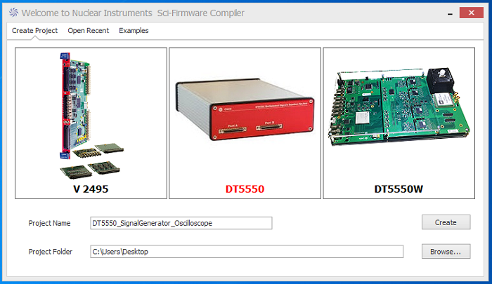
Create the project. Run Sci-Compiler and in the starting window click on the DT5550 button, write a name for the project in the “project Name” field, write a destination path for the project in the “Project Folder” field (or search the folder with the “Browse…” button) and click the “Create” button.
-
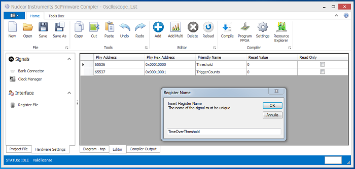
Create the Registers. Three registers will be implemented to allow the user to change the threshold of the Leading Edge Trigger and to read the total number of trigger signals and the event by event time over threshold.Click the “Memory Mapping” tab on the bottom tab menu. Then enter the name of the register and click add. Repeat the operation to create the “Threshold”, the “TriggerCounts” and the “TimeOverThreshold” registers.
-
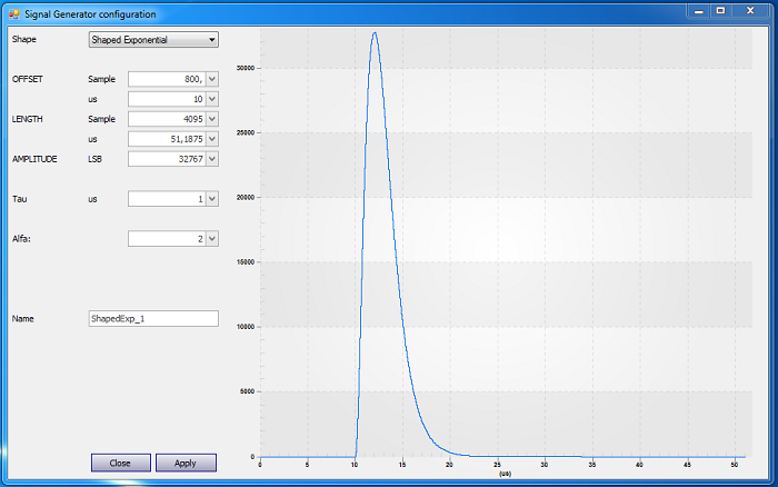
Add the Signal Generator. Select the “Tools Box” toolbar and click the “Delay Memory” button in the “Logic” group. In the sub menu click on “Signal Generator”. A configuration window will appear: set the parameters as shown in the following figure, selecting the “Shaped exponential” in the “Shape” menu, change the “OFFSET” by writing 800 in the correspondent “Sample” field and insert a name in the “Name” field. Click the “Apply” button to close the window and add the Signal Generator block to the diagram.
-
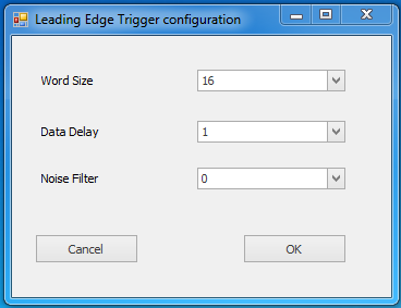
Add the Leading Edge Trigger. Click the “DAQ” button in the “Signal Processing” group of the “Tools Box” toolbar. In the sub menu click the “Trigger (Leading Edge)” and in the configuration window set the parameters as shown in the following figure. Then click “OK” to create the block in the diagram.
Connect the “OUT” output pin of the Signal Generator block to the “In” pin of the Trigger block to generate a trigger signal when the generated shaped exponential signal exceeds a threshold. In order to provide the threshold, click the “Register” menu, select the “Register (Read)” item and the following window will be displayed:
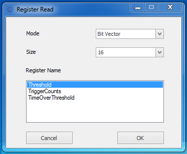
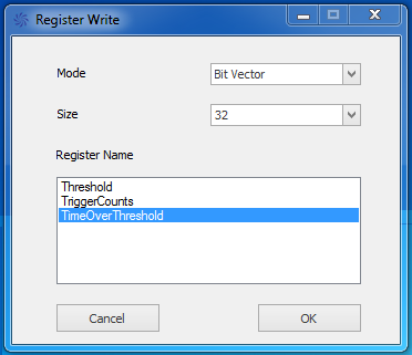
Select the “Threshold” register and choose the Bit Vector option for the “Mode” field and the value 16 for the “Size” field. Click “OK” and the correspondent register block will be added to the diagram. Connect the “Threshold” output pin of the register block to the “Threshold” input signal of the Trigger block.
-
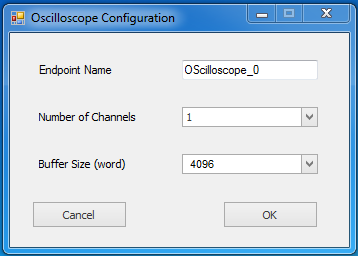
Add the Oscilloscope. In the “DAQ” sub menus click the “Oscilloscope” and in the correspondent configuration window choose the value 1 for the “Number of Channels” field and the value 4096 for the “Buffer size” field to match the number of samples of the generated signal. Click the “OK” button to add the oscilloscope block to the diagram. Then connect the “OUT” output pin of the Signal Generator to the “A1” analog input pin of the Oscilloscope to see the generated signal. The “TOT” output pin of the Trigger has to be linked to the “D0 1” digital input pin of the Oscilloscope to see the time over threshold signal.
-
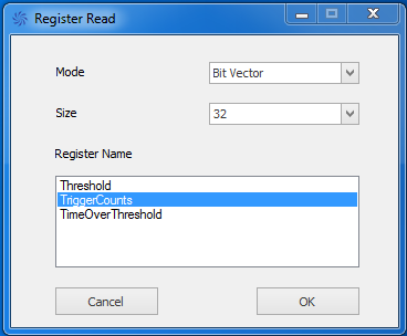
Add the Counter. In order to count the number of trigger signals click the “Timer Counters” in the “Logic” group and select the Counter item to add the block to the diagram. Connect then the “Trigger” output pin of the Trigger block to the “In” input pin of the Counter block. In order to keep the signal counting enabled click the “Misc” button, choose the “True” item and connect the output of the block that has been created in the diagram to the “GATE” input of the Counter block. The number of counts is available at the “Counts” output of the block and can be read by the user with the correspondent register. Click the “Register” menu, select the “Register (Write)” item and in the following window select the “TriggerCounts” register and choose in the “Mode” menu the Bit Vector option and in the “Size” menu the 32 value. Click “OK” and connect the “Counts” output of the Counter to the “TriggerCounts” input of the register. In order to enable the writing of the value in the register, connect the “True” block that has been already created to the “WR” input of the register.
-
Add the Chronometer. The “TOT” output signal of the Trigger is a signal that stays high if the input signal exceeds the threshold. In order to measure the number of clock for which the “TOT” is high a Chronometer can be used. Click the “Timer Counters” menu of the “Logic” group and select the “Chronometer (Start Stop)” item to add the block to the diagram. Add to the diagram also the “Edge Detector (Rising Edge)” and the “Edge Detector (Falling Edge)” by clicking the correspondent items in the “Sequential Logic” menu. Connect then the “TOT” output of the Trigger to the “In” inputs of both the Rising and the Falling Edge Detector blocks and feed their “OUT” output signals respectively to the “Start” and “Stop” input pin of the Chronometer block. Create a constant integer of value 1 by clicking the “Misc” menu, selecting the “Constant (int)” item and inserting the number 1 in the configuration window. Connect the output of the generated block to the “Pulse Width” input of both the Edge Detectors to specify that the output block length corresponds to a single clock cycle. The Chronometer counts the clock cycles occurring between the start and stop signal and provides it to the “Time” output pin. The value can be read by adding a register: click the “Register (Write)” in the “Register” menu of the “Communication” group, select the “TimeOverThreshold” register and set Bit Vector as “Mode” and 32 as “Size”.
Connect then the “Time” output of the Chronometer block and the “True” block respectively to the “TimeOverThreshold” input and to the “WR” input of the register block. Finally, the time value measured by the Chronometer has to be reset at each event: for this purpose the “Trigger” output of the Trigger block can be fed to the “Reset” input of the Chronometer block.
-
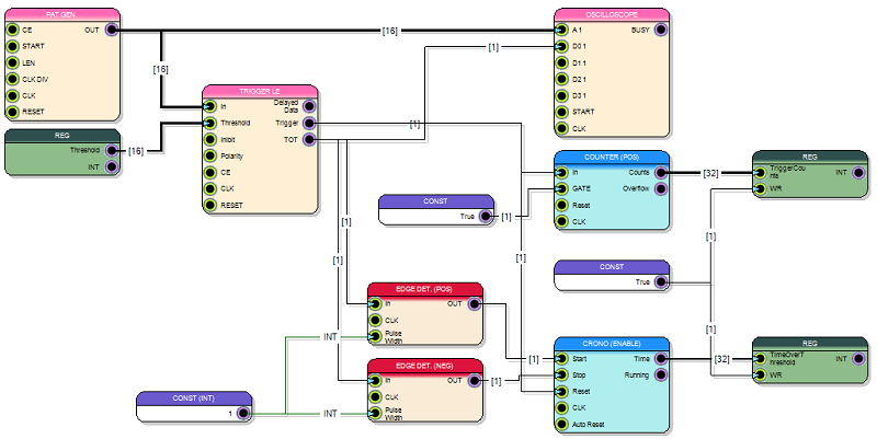
Compile the project. The firmware is completed and the diagram should look as the one displayed in the following picture.
Select the “Home” toolbar and press the “Compile” button. The Sci-Compiler executes the firmware compilation by running Vivado and redirecting the output in the “Compiler Output” tab. At the end of the process, when the .bit file has been created, the text “Successful Compilation!” is shown in the output.
-
Program the FPGA. For this step the DT5550 board should be powered on and connected to the computer through one of the supported cables, as explained in the FPGA Programming section. Then press the “Program FPGA” button to automatically connect to the cable and then to the FPGA and download the generated firmware. The text “Target device programmed successfully” that appears in the “Compiler Output” states the end of the process.
-
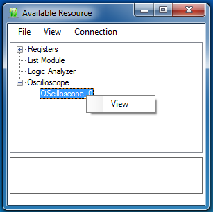
Test the firmware. The generated firmware can be tested by using the Resource Explorer tool. Click the “Resource Explorer” button and in the “Connection” window select the DT5550 board, the desired “Connection Type” and the correct “Serial Number” or “IP”. The “Select Json File” will be automatically filled with path of the .json file created during the firmware compilation process. By clicking the “Connect” button the connection with the board will be established. In the following window it will be shown the resources available on the FPGA (Registers, List Modules, Logic Analyzers and Oscilloscopes).
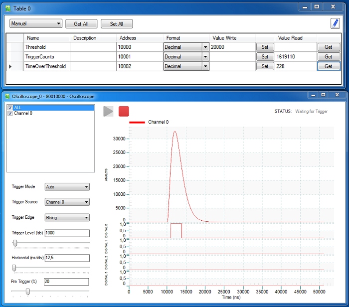
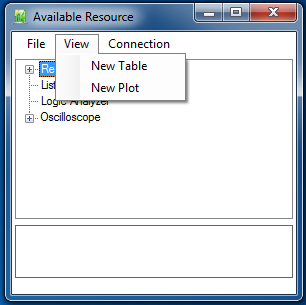
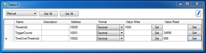
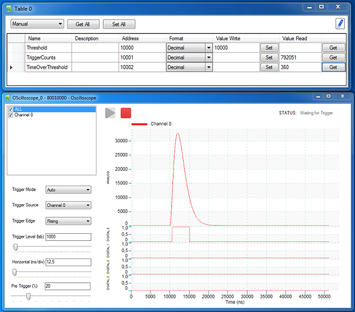
Click the “View” menu and create a table to control the registers by clicking the “New Table” button. The “Table 0” will be created and shown.
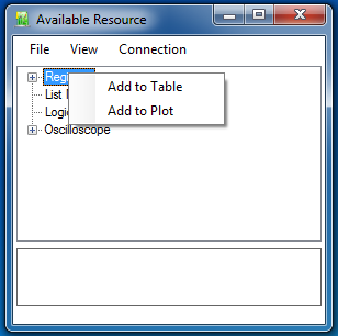
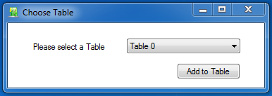
Then click with the right button of the mouse on “Registers” and click the “Add All to Table” button: select the “Table 0” in the Choose Table window and click the “Add to Table” button. The three registers will be added to the table, each one with its name and address.
Write the value 1000 in the “Value Write” cell of the “Threshold” row and click the “Set” button to write the value into the correspondent register (be sure that the “Format” is set to “Decimal”). The user can read the number of trigger signals and the number of clock cycles corresponding to the time over threshold in the “Value Read” cell of the correspondent registers by clicking on the “Get” buttons. Considering the clock frequency used on the board i.e. 80 MHz, the time over threshold corresponds to about 8200 ns.
Right click on the oscilloscope item (Oscilloscope_0) and press the “View” button to open the oscilloscope window.
The title of the window contains the name of the oscilloscope and its address. In the box on the left it is possible to choose the channels to be visualized by clicking the correspondent checkbox. Selecting a channel, all the connected signals (analog and four digital) will be displayed with the same color. Set as “Trigger Mode” the “Single” item to visualize a single wave and the “Channel 0” as “Trigger Source”. In this case the oscilloscope trigger for the signal monitoring is a leading edge trigger on the analog signal: the “Trigger Edge” should be specified to be “Rising” and the “Trigger Level” could be set to 1000 lsb. By clicking the green arrow, the waveform acquisition starts and the analog signal and its time over threshold are displayed on the plot (the amplitude of the digital signals is set to be equal to the maximum of the analog signal). it is possible to see that the length of the time over threshold signal is exactly 8200 ns.
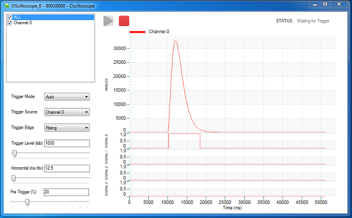
It is possible to notice that by setting 10000 lsb as trigger level in the “Threshold” register the number of cycles of the “TimeOverThreshold” register is 360, which means 4500 ns, corresponding to the length of the time over threshold signal on the oscilloscope plot.
By increasing the value set in the “Threshold” register to 20000 lsb it is possible to read in the “TimeOverThreshold” register a value of 228 clock cycles, corresponding to 2850 ns, as shown in the oscilloscope plot.