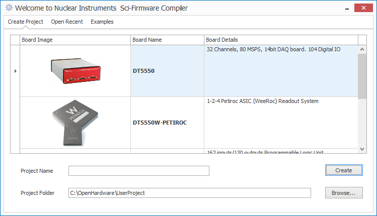
Create the project. Run Sci-Compiler and in the starting window click on the V2495 button, write a name for the project in the “project Name” field, write a destination path for the project in the “Project Folder” field (or search the folder with the “Browse…” button) and click the “Create” button.
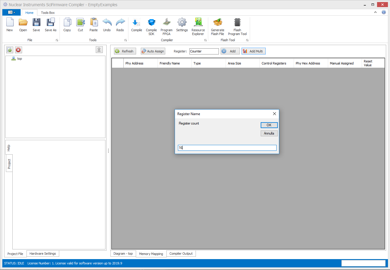
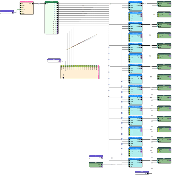
Create the Registers. Sixteen Registers allow the user to read the number of signals in each channel and an additional register will be used to reset the value of all the other registers at the same time. Click the “Memory Mapping” tab on the bottom tab menu. Then enter the name of the register group in the Register filed and click the “Add Multi” button .
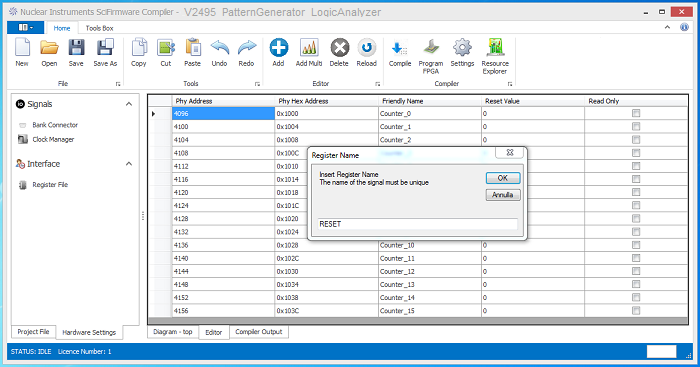
Clicking the “OK” button another window will appear to ask the number of registers to be added: insert 16 and click the “OK” button. The registers will be automatically created with a name containing an incremental value, as can be seen in the table of the “Editor” tab.
Then, Enter “RESET” as register name and click the “Add”.
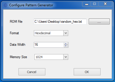
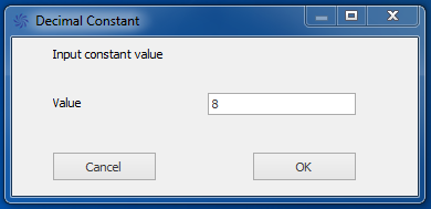
Add the Pattern Generator. First create a file containing a list of random numbers from 0 to 65535 expressed with the hexadecimal notation, that will be used as a source for the Pattern Generator block. Then select the “Tools Box” toolbar and click the “Delay Memory” button in the “Logic” group. In the sub menu click on “Pattern Generator”. A configuration window will appear: in the “ROM File” field write the path of the file of random numbers (or click the correspondent button to search the file in the computer), select the “Hexadecimal” option for the “Format”, the value 16 for the “Data Width” and the value 1024 for the “Memory Size”. Click the “OK” button to close the window and add the Pattern Generator block to the diagram. In order to slow down the data generation click the “Misc” button in the “Wire” group, select “Constant (INT)”, write 8 in the “Value” field of the appearing window, click “OK” and connect the block that has been created on the diagram to the “CLK DIV” input of the Pattern Generator block.
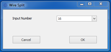
Add the Wire Split. In order to create 16 different random digital signals, the output of the Pattern Generator has to be split in 16 single bits. Click the “Wire Split” item of the “Binary Operations” sub-menu in the “Wire” group of the “Tools Box” toolbar. In the following window select the value 16 and click the “OK” button. Connect the “OUT” output pin of the Pattern Generator block to the “IN” input pin of the created Wire Split block.
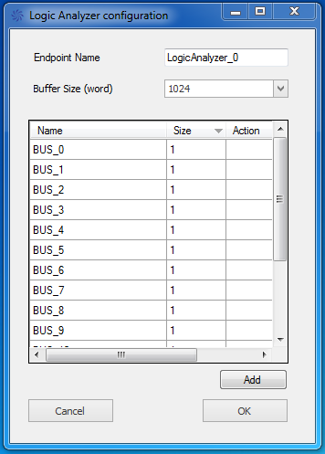
Add the Logic Analyzer. The Logic Analyzer block will allow the user to display the 16 digital signals through the correspondent tool in the Resource Explorer. Click the “DAQ” button in the “Signal Processing” group and select the “Logic Analyzer” button from the sub-menu. A configuration window will be shown: choose the value 1024 for the “Buffer Size (word)”, click the “Add” button for 16 times in order to create 16 channels with size 1 and then press “OK” to add the block to the diagram.
Connect each output pin of the Wire Split block to an input pin of the Logic Analyzer block: the “alt + r” shortcut can be used to make the operation faster (create the first link, select it, press the combination of characters and insert the value 15 in the window that will appear to automatically create the links).
Create a True constant by clicking the correspondent item in the “Misc” sub-menu of the “Wire” group. Connect the True block to the “TRIGGER” input of the Logic Analyzer block to ensure the presence of a trigger when operating with the external trigger.
Add the Counters. In order to count the number of signals in each channel, 16 Rising Edge Counters has to be added by clicking the correspondent item in the “Timer Counters” sub-menu in the “Logic” group (once a block has been created, copy and paste it to speed up the operation). Connect each output pin of the Wire Split block to the “in” input of a Counter block: create the first link, press “alt + f” and then click on all the destination blocks.
Create another True constant and connect it at the “GATE” input of each Counter block: create a first link, select it, press “alt + e” and click on all the Counter blocks to automatically create the links.
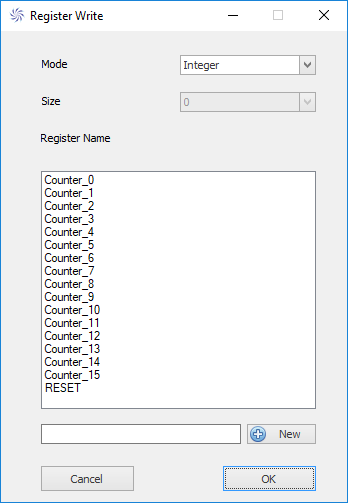
Add the Registers. Click the “Register” button in the “Communication” group and select the “Register Write” item. In the window that will be shown select all the counter registers and set the “Mode” to “Bit Vector” and the “Size” to 32. By clicking the “OK” button the 16 Registers will be added to the diagram. Connect the “Counts” output of each Counter block to the correspondent Register using the “alt + s” shortcut: select the first link, use the character combination and then click one by one the Counter blocks. Create a True constant and connect it at the “WR” input of each Register block using the “alt + e” shortcut. In order to reset the value of each Counter block click in the “Register” sub-menu the “Register Read”, select the “RESET” Register, set it as a “Bit Vector” of size 1 and press “OK”. Connect the Register block to each “Reset” input of the Counter blocks, speeding up the operation by using the “alt + e” characters combination.
Compile the project. The firmware is completed and the diagram should look as the one displayed in the following picture.
Select the “Home” toolbar and press the “Compile” button. The Sci-Compiler executes the firmware compilation by running Quartus and redirecting the output in the “Compiler Output” tab. At the end of the process, when the .rpd file has been created, the text “Successful Compilation!” is shown in the output.
Program the FPGA. For this step the V2495 board should be powered on and connected to the computer through one of the supported cables, as explained in the FPGA Programming section. Then press the “Program FPGA” button to automatically connect to the cable and then to the FPGA and download the generated firmware. The text “Target device programmed successfully” that appears in the “Compiler Output” states the end of the process.
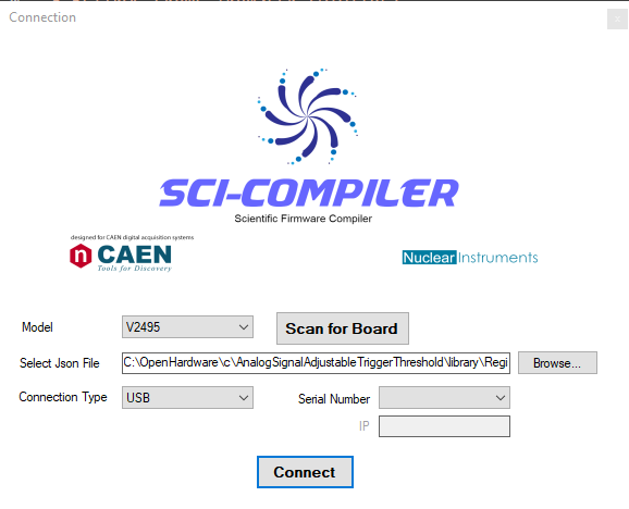
Test the firmware. The generated firmware can be tested by using the Resource Explorer tool. Click the “Resource Explorer” button and in the “Connection” window select the V2495 board, the desired “Connection Type” and the correct “Serial Number” or “IP”. The “Select Json File” will be automatically filled with path of the .json file created during the firmware compilation process. By clicking the “Connect” button the connection with the board will be established. In the following window it will be shown the resources available on the FPGA (Registers, List Modules, Logic Analyzers and Oscilloscopes).
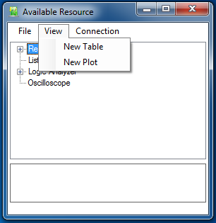
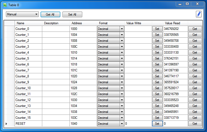
Click the “View” menu and create a table to control the registers by clicking the “New Table” button. The “Table 0” will be created and shown.
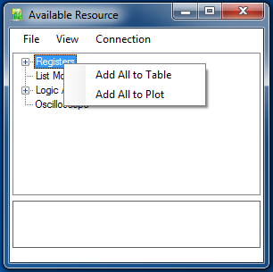
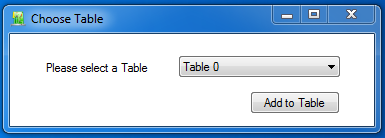
Then click with the right button of the mouse on “Registers” and click the “Add All to Table” button: select the “Table 0” in the Choose Table window and click the “Add to Table” button. All the registers will be added to the table, each one with its name and address.
In order to read the value of each register it is sufficient to click the “Get All” button, as shown in the following window. In order to continuously update the values, choose one of the available option between “Auto 50 ms”, “Auto 100 ms”, “Auto 500 ms”, “Auto 50 ms”, “Auto 1 s”, “Auto 10 s” to set the automatic refresh time (instead of “Manual”).
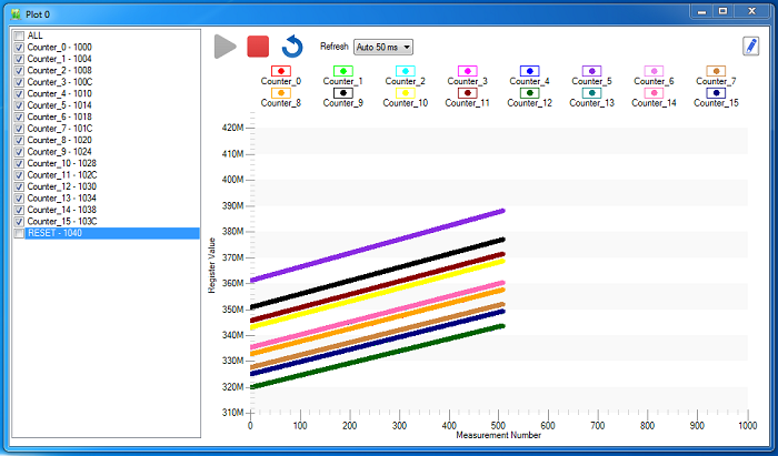
A graphical way to access the Registers value is the Plot tool. Click the “View” menu and then the “New Plot” button. The “Plot 0” will be created and shown.
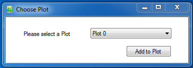
Right click on “Registers” and click the “Add All to Plot” button: select the “Plot 0” in the Choose Plot window and click the “Add to Plot” button.
All the Registers will be added to the list on the left of the plot, each one with its name and address. In order to add a Register value to the plot the correspondent checkbox has to be flagged. The “ALL” checkbox will automatically check or uncheck all the Registers of the list. Select an option for the “Refresh” and click the
button to start the acquisition. The
button will be used to stop the acquisition, while the
button will delete all the data.
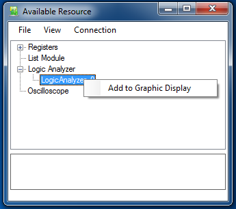
In order to visualize the 16 digital signals the user has to right click on the “LogicAnalyzer_0” item and press “Add toGraphic Display”.
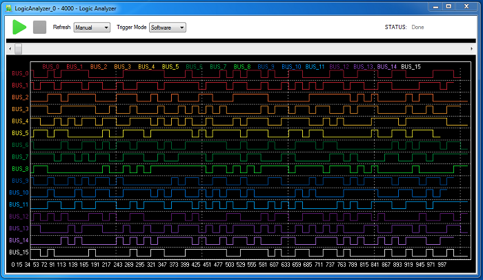
The title of the window that will be shown contains the name and the address of the block. Select the “Manual” or the “Auto” option for the “Refresh” to respectively manually or automatically update the data in the graphic. The “Trigger Mode” should be set to “Software” to go in a free running mode or to “Signal” to use as a trigger the “TRIGGER” input of the Logic Analyzer block (which is always set to 1 in this example). Click the
button to start the acquisition: the 16 buffers containing the digital signals will be displayed with different colors. The
button will be used to stop the acquisition.